
Open now · until 4 PM
1-800-321-5031
ADVANCED MICRO DEVICES

AM29LV008BB-90EC

NOR Flash Parallel 3V/3.3V 8M-bit 1M x 8 90ns 40-Pin TSOP

In stock: 2,900

On our shelves in San Jose. We do not dropship.

Stock on our shelves

Date code and country of origin on every lot.

Lots in stock for AM29LV008BB-90EC
Quantity Date code Country of origin
1,742 0915 United States
905 0746 United States
253 1997 United States
2,900 3 lots on the shelf

Need a specific date code, or all of it from a single lot? Tell us on the quote and we will confirm before shipping.

Specifications

Manufacturer ADVANCED MICRO DEVICES
Manufacturer part number AM29LV008BB-90EC
Our part number 506596
Category IC
Description NOR Flash Parallel 3V/3.3V 8M-bit 1M x 8 90ns 40-Pin TSOP
Date codes in stock 0746, 0915, 1997
Datasheet

Compliance & export

ECCN EAR99
Country of origin United States

Classification is provided for reference and confirmed on the invoice. Certificate of conformance and date-code guarantee on request — ask with your order.

Description

AM29LV008BB-90EC AMD AM29LV008BB90EC NOR Flash Parallel 3V/3.3V 8M-bit 1M x 8 90ns 40-Pin TSOP 120 X TRAY OBSOLETESKU 00506596 The Am29LV008B is an 8 Mbit, 3.0 volt-only Flash memory organized as 1,048,576 bytes. The device is offered in a 40-pin TSOP package. The byte-wide (x8) data appears on DQ7DQ0. This device requires only a single, 3.0 volt VCC supply to perform read, program, and erase operations. A standard EPROM programmer can also be used to program and erase the device. This device is manufactured using AMD's 0.32 um process technology, and offers all the features and benefits of the Am29LV008, which was manufactured using 0.5 um process technology. In addition, the Am29LV008B features unlock bypass programming and in-system sector protection/unprotection. The standard device offers access times of 70, 90, and 120 ns, allowing high speed microprocessors to operate without wait states. To eliminate bus contention the device has separate chip enable (CE#), write enable (WE#) and output enable (OE#) controls. The device requires only a single 3.0 volt power supply for both read and write functions. Internally generated and regulated voltages are provided for the program and erase operations. The device is entirely command set compatible with the JEDEC single-power-supply Flash standard. Commands are written to the command register using standard microprocessor write timings. Register contents serve as input to an internal state-machine that controls the erase and programming circuitry. Write cycles also internally latch addresses and data needed for the programming and erase operations. Reading data out of the device is similar to reading from other Flash or EPROM devices. Device programming occurs by executing the program command sequence. This initiates the Embedded Program algorithm"an internal algorithm that automatically times the program pulse widths and verifies proper cell margin. The Unlock Bypass mode facilitates faster programming times by requiring only two write cycles to program data instead of four. Device erasure occurs by executing the erase command sequence. This initiates the Embedded Erase algorithm"an internal algorithm that automatically preprograms the array (if it is not already programmed) before executing the erase operation. During erase, the device automatically times the erase pulse widths and verifies proper cell margin. The host system can detect whether a program or erase operation is complete by observing the RY/BY# pin, or by reading the DQ7 (Data# Polling) and DQ6 (toggle) status bits. After a program or erase cycle has been completed, the device is ready to read array data or accept another command. The sector erase architecture allows memory sectors to be erased and reprogrammed without affecting the data contents of other sectors. The device is fully erased when shipped from the factory. Hardware data protection measures include a low VCC detector that automatically inhibits write operations during power transitions. The hardware sector protection feature disables both program and erase operations in any combination of the sectors of memory. This can be achieved in-system or via programming equipment. The Erase Suspend feature enables the user to put erase on hold for any period of time to read data from, or program data to, any sector that is not selected for erasure. True background erase can thus be achieved. The hardware RESET# pin terminates any operation in progress and resets the internal state machine to reading array data. The RESET# pin may be tied to the system reset circuitry. A system reset would thus also reset the device, enabling the system microprocessor to read the boot-up firmware from the Flash memory. The device offers two power-saving features. When addresses have been stable for a specified amount of time, the device enters the automatic sleep mode. The system can also place the device into the standby mode. Power consumption is greatly reduced in both these modes. AMD's Flash technology combines years of Flash memory manufacturing experience to produce the highest levels of quality, reliability and cost effectiveness. The device electrically erases all bits within a sector simultaneously via Fowler-Nordheim tunneling. The data is programmed using hot electron injection.

Similar parts on our shelves

Same part number family — confirm the specs before you swap.

ADVANCED MICRO DEVICES

AM29LV800BB-90EC

Only 96 left
$4.3500 / ea

ADVANCED MICRO DEVICES

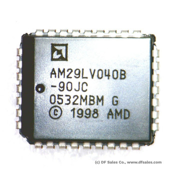
AM29LV040B-90JC

AM29LV040B-90JC AMD EPROM NOR FLASH 4Mb SOJ

Only 60 left
$2.0000 / ea