K9F1G08U0A-PIB0
Ask for availability
$6.0000
/ ea

In stock and available to order. 653 results.
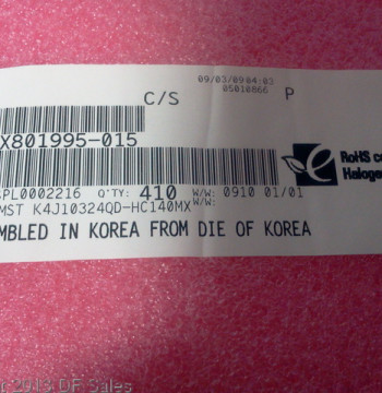
K4S561632B-TC75 K4S561632B-TC75000 SDRAM 256BIT 133MHZ 4MX16
Only 17 leftDRAM Chip EDO DRAM 16Mbit 1Mx16 5V 42-Pin SOJ K4E151611DJC60
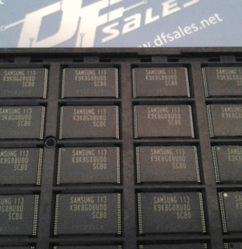
In stock: 101K9K4G08U0M-PCB0 SAMSUNG K9K4G08U0MPCB0 K9K4G08U0M-PCB0000 SLC NAND Flash Parallel 3.3V 4G-bit 512M x 8 25us 48-Pin TSOP-I Offered in 512Mx8bit or 256Mx16bit, the K9K4GXXX0M is 4G bit with spare 128M bit capacity. Its NAND cell provides the most cost-effective solution for the solid state mass storage market. A program operation can be performed in typical 300ms on the 2112- byte(X8 device) or 1056-word(X16 device) page and an erase operation can be performed in typical 2ms on a 128K-byte(X8 device) or 64K-word(X16 device) block. Data in the data page can be read out at 50ns cycle time per byte. The I/O pins serve as the ports for address and data input/output as well as command input. The on-chip write controller automates all program and erase functions including pulse repetition, where required, and internal verification and margining of data. Even the write-intensive systems can take advantage of the K9K4GXXX0M¢s extended reliability of 100K program/erase cycles by providing ECC(Error Correcting Code) with real time mapping-out algorithm. The K9K4GXXX0M is an optimum solution for large nonvolatile storage applications such as solid state file storage and other portable applications requiring non-volatility.
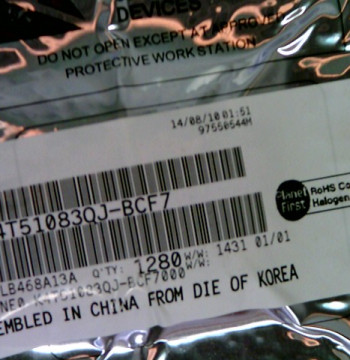
Ask for availabilityK4T51083QJ-BCF7 DRAM Chip DDR2 SDRAM 512Mbit 64Mx8 1.8V 60-Pin FBGA 512Mb J-die DDR2 SDRAM60 & 84FBGA with Lead-Free & Halogen-FreeRoHS compliant
In stock: 1,182KM68B1002J-8TAPE
In stock: 101KM416C1200BJ-6DRAM Chip FPM 16Mbit 1Mx16 5V 42-Pin SOJCUT TAPE OBSOLETE
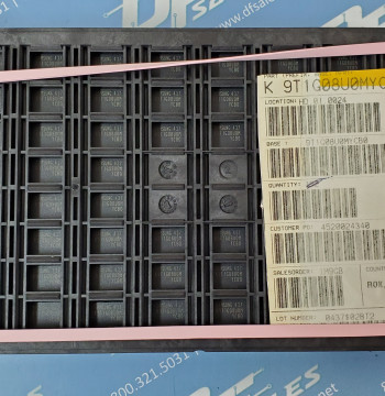
Only 49 leftK9T1G08U0MYCB0 SAMSUNG K9T1G08U0M-YCB0 SLC NAND Flash Parallel 3.3V 1G-bit 128M x 8 15us 48-Pin TSOP-I 96 X TRAY OBSOLETE The K9T1G08U0M is a 1,056Mbits(1,107,296,256 bits) memory organized as 262,144 rows(pages) by 528 columns. Spare sixteen columns are located from column address of 512 to 527. A 528-bytes data register is connected to memory cell arrays accommodating data transfer between the I/O buffers and memory during page read and page program operations. The memory array is made up of 16 cells that are serially connected to form a NAND structure. Each of the 16 cells resides in a different page. A block consists of the 32 pages formed two NAND structures. A NAND structure consists of 16 cells. Total 8,448 NAND structures reside in a block. The array organization is shown in Figure 2. The program and read operations are executed on a page basis, while the erase operation is executed on a block basis. The memory array consists of 8,192 separately erasable 16K-bytes blocks. It indicates that the bit by bit erase operation is prohibited on the K9T1G08U0M. The K9T1G08U0M has addresses multiplexed into 8 I/O's. This scheme dramatically reduces pin counts and allows systems upgrades to future densities by maintaining consistency in system board design. Command, address and data are all written through I/O's by bringing WE to low while CE is low. Data is latched on the rising edge of WE. Command Latch Enable(CLE) and Address Latch Enable(ALE) are used to multiplex command and address respectively, via the I/O pins. The 128M byte physical space requires 27 addresses, thereby requiring four cycles for byte-level addressing : 1 cycle of column address, 3 cycles of row address, in that order. Page Read and Page Program need the same four address cycles following the required command input. In Block Erase operation, however, only the 3 cycles of row address are used. Device operations are selected by writing specific commands into the command register. Table 1 defines the specific commands of the K9T1G08U0M. The device provides simultaneous program/erase capability up to four pages/blocks. By dividing the memory array into four 256Mbit separate planes, simultaneous multi-plane operation dramatically increases program/erase performance by 4X while still maintaining the conventional 512 bytes structure. The extended pass/fail status for multi-plane program/erase allows system software to quickly identify the failing page/block out of selected multiple pages/blocks. Usage of multi-plane operations will be described further throughout this document. In addition to the enhanced architecture and interface, the device incorporates copy-back program feature from one page to another of the same plane without the need for transporting the data to and from the external buffer memory. Since the time-consuming burstreading and data-input cycles are removed, system performance for solid-state disk application is significantly increased. The device includes one block sized OTP(One Time Programmable), which can be used to increase system security or to provide identification capabilities. Detailed information can be obtained by contact with Samsung.
Ask for availabilityIC MEM 32GB LPDDR4X 200FB
Ask for availabilityK6F2008V2E-YF70SRAM Chip Async Single 3.3V 2M-bit 256K x 8 70ns 32-Pin TSOP-IOBSOLETE
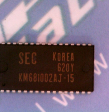
Only 35 leftKM681002AJ-15 KM681002AJ15 128K X 8 STANDARD SRAM 22 X TUBE
In stock: 144K6T4008C1B-GF70SRAM Chip Async Single 5V 4M-bit 512K x 8 70ns 32-PinOBSOLETE
Ask for availabilityNot the part you needed?
Not all of our inventory is listed online. Send us the exact number and quantity.
Request a Quote